
By rapidly twisting a microscopically small tip back and forth, researchers at the University of Maryland (UMD) have unlocked a new way to detect subtle changes on the surface of a material flexing in response to infrared light.
In a paper published Aug. 5, 2026 in the journal Nature Communications, the researchers describe a new way to take high-resolution images that they call infrared torsional force microscopy, or TFM-IR for short. It allows them to measure the surface of a material with near-nanometer precision as it stretches and warps in response to infrared light—invisible light readily absorbed by many kinds of chemical bonds that causes them to vibrate. It’s the first technique that can measure both the vertical and horizontal vibrations induced by light with such high precision.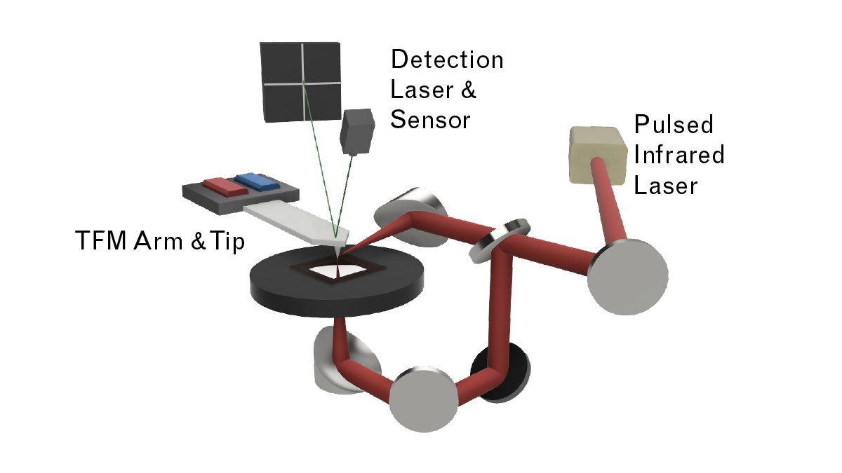 Caption: A schematic of a novel infrared torsional force microscopy (TFM-IR) experiment conducted at the University of Maryland. A material sample (located on the dark gray disc) is illuminated with pulses from an infrared laser. A microscopic tip, twisted rapidly back and forth on a long arm, scans the surface of the material to sense its response to the light. A second laser is bounced off the arm to measure small changes to its twisting motion, allowing researchers to capture a detailed image of the sample's surface. (Schematic courtesy of the authors.)
“We have overcome a long-standing limitation in optical imaging,” says Min Ouyang, a professor of physics at UMD and a member of the Quantum Materials Center and the Maryland NanoCenter who led the new project. “Modern quantum materials derive many remarkable properties from variation that happens over distances of only a few nanometers, or even less. Conventional optical microscopes cannot really resolve this.”
The method Ouyang and his colleagues developed builds on atomic force microscopy (AFM), which was first developed in the 1980s and has matured into a standard technique for measuring the surfaces of material samples with extreme precision. Unlike traditional microscopes, AFM works more like your fingertips than your eyes. Instead of creating an image by collecting light with a lens, AFM drags a tiny tip across a material to feel the forces from its bumps and ridges. The technique can spot features that are smaller than a nanometer and, under the right conditions, can even resolve individual atoms.
By itself, AFM only sees the topography of a surface: It can sense that it’s higher over here and lower over there, but it doesn’t provide any details about the chemical composition of a sample. To learn about the makeup of a material, researchers often excite vibrations in a sample with infrared light and use the AFM tip to sense how the surface changes. Because chemical bonds respond in predictable ways to infrared light, the combination of AFM and infrared light can identify the signatures of particular molecules, either to verify the composition of a sample or to detect the presence of unwanted contaminants.
“If you shine some light on your sample, you're going to get some very slight thermal expansion,” says Yonatan Gazit, a graduate student in physics at UMD who is also the lead author of the new paper. “AFM is essentially measuring that thermal expansion to understand how well your sample is absorbing or interacting with the light.”
Modern AFM devices feature a sharp tip suspended above a sample on the underside of a skinny arm. Electronics rapidly drive the arm up and down, which gently taps the tip against the sample at a regular rhythm. The tapping helps the tip avoid getting stuck on a ridge, which would potentially damage material being studied, and enhances the sensitivity to infrared vibrations by closely matching their frequency. As the tip traverses the surface, the rhythmic tapping is altered as the material flexes and pushes against it. Researchers measure these subtle changes in tapping frequency by bouncing laser light off the top of the vibrating arm to monitor its motion.
The tapping technique is excellent for making sensitive measurements of height, but it doesn’t do a good job sensing how a material expands or contracts horizontally. In a paper published in 2024 in the Proceedings of the National Academy of Sciences, a team from Stanford University and their colleagues showed that twisting the AFM tip at a regular frequency instead of tapping it could measure previously undetectable variations along the surface of a double-decker stack of graphene, formed from two stacked layers of carbon atoms each arranged in a honeycomb pattern of repeating hexagons. They named their technique torsional force microscopy (TFM).
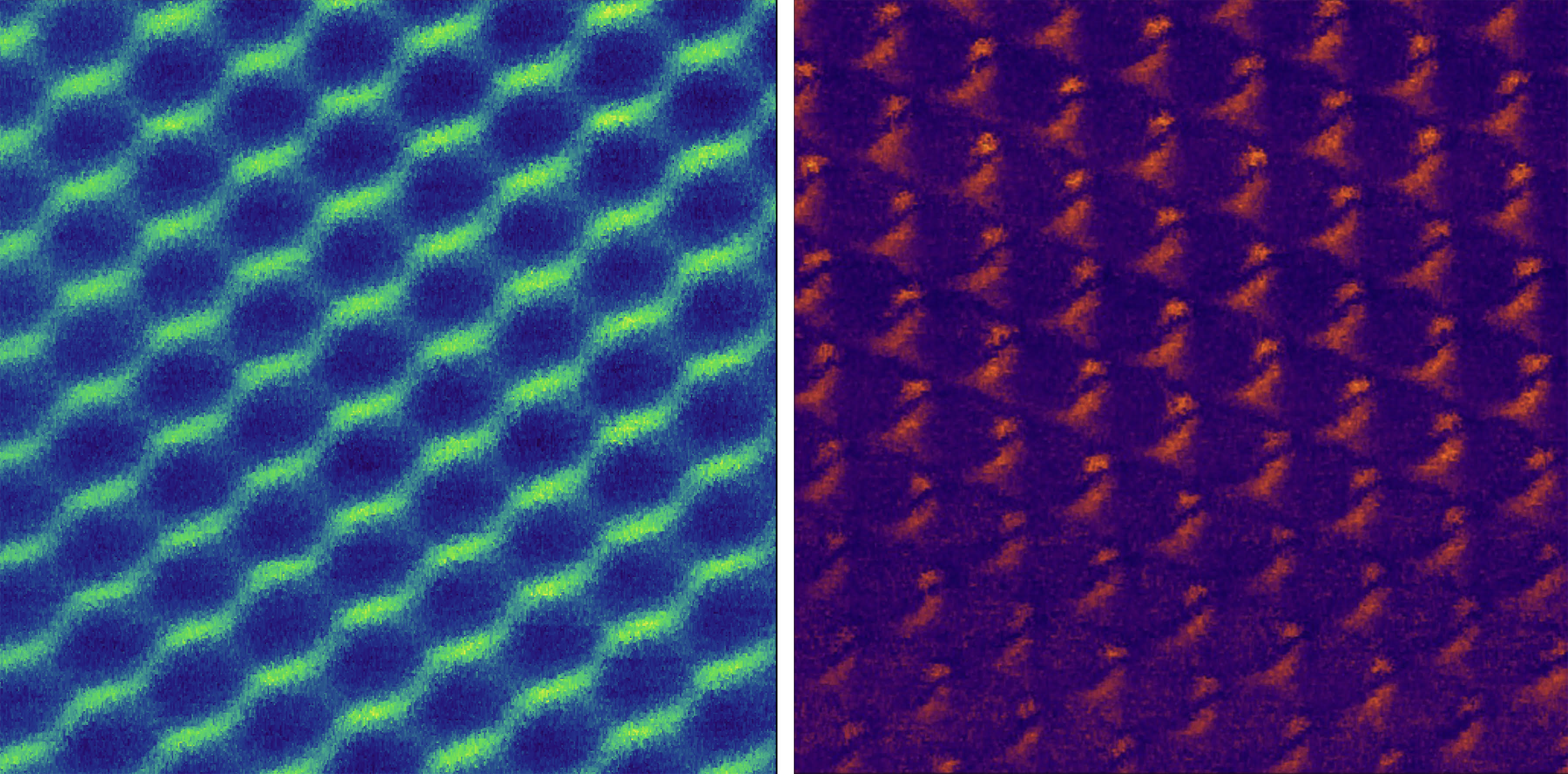 Caption: Two torsional force microscopy (TFM) images of bilayer graphene. On the left, standard TFM captures the material's signature honeycomb lattice. On the right, the new method (TFM-IR) captures much more detail about how the chemistry of the surface responds to infrared light. (Images courtesy of the authors.)Inspired by this result, Gazit, Ouyang and their colleagues designed an experiment that combined infrared illumination with the twisting technique. As the tip twists back and forth, pulses from an infrared laser periodically wash over a small sample of a material. Some energy from each pulse gets absorbed by the material, causing it to swell and vibrate. Choosing the frequency of the pulses—that is, how many pulses arrive at the sample per second— enables the tip to pick out either the vertical changes or the horizontal changes, similar to how a strobe light can selectively pick out or freeze certain kinds of motion.
As a proof of concept, the researchers tested the new technique by studying the surface of a small piece of mica, a shiny and flaky mineral used in manufacturing everything from drywall to tires to fireproof material for industrial ovens. They chose mica both because it’s already well-understood and because the chemical bonds that hold it together point along different directions, making it a good candidate for measuring both the vertical and horizontal vibrations induced by infrared light.
The team showed that they could detect four vibration patterns in mica and demonstrated that they could distinguish the horizontal and vertical movement by using different infrared laser pulse rates. They zeroed in on a small bump—a mica nanobubble on the surface just a few nanometers tall—and carefully dragged the tip from the center of the bump to its edge. They compared the results of their measurements with simulations of the horizontal and vertical vibrations expected from the way the bubble strained and bulged, and they found that the locations of the strongest horizontal and vertical responses to infrared light lined up between theory and experiment.
The team next turned their attention toward a double layer of graphene, the same material studied in the paper that first introduced the torsional technique. On its own, graphene has intrigued scientists for more than two decades because of its unique electrical and mechanical properties. When it’s stacked into two layers, with one layer rotated by a small amount, it gets even more interesting. The two layers form what’s called a moiré material, and in 2018, researchers found that a very particular angle turned a moiré stacking of graphene into a perfect electrical conductor—a quantum effect that made the material a superconductor.
Researchers remained in the dark about the microscopic origins of the effect. Because a moiré material is only a couple of atoms thick, the tiny changes in the lattice that give rise to its remarkable properties cannot be revealed by simply scanning its height. The torsional trick introduced in 2024 pointed toward a new way to image these atomically thin materials.
In the new paper, the team examined a sample comprising two layers of graphene stacked together at a small angle. They compared a standard TFM image of the sample with an image taken using their TFM-IR approach—both taken of the same exact sample at the exact same spot. The standard TFM image clearly showed the material’s signature lattice of hexagons, but the TFM-IR image revealed a wealth of additional details. Instead of merely showing the shape of the lattice, TFM-IR showed for the first time how different chemical bonds in a single hexagon—including bonds within a single sheet of graphene and bonds between the two sheets—react to infrared light, revealing a unique vibrational fingerprint of the underlying material. Understanding this fingerprint and the way that it changes when the stacking angle changes could prove crucial to gaining a better understanding of moiré materials and their properties.
“Our technique combines three capabilities that are rarely available in a single measurement,” Ouyang says. “First, it brings optical imaging and spectroscopy to the nanoscale, providing spatial resolution down to nearly one nanometer. Second, it can distinguish directional responses within a material, allowing us to uncover anisotropic properties that conventional techniques cannot resolve, Third, it provides each material’s unique spectroscopic fingerprint. In other words, our technique doesn’t just show what a material looks like; it also identifies what it is and reveals the hidden physical processes that govern its behavior by mapping how it responds to light with nanometer-scale precision.”
Ouyang and the team hope that the technique will be a key tool in characterizing and even designing materials going forward, and they emphasize that it has the added benefit of working at room temperature. In particular, TFM-IR might be useful for semiconductor companies, who are on the hunt for techniques to spot defects in their chips. The authors say that a technique capable of mapping the mechanical signatures of local chemistry could guide the development of new advanced manufacturing processes and might even help researchers optimize next-generation nanoscale devices, including quantum sensors and photonic quantum computers.
Story by Chris Cesare
In addition to Ouyang and Gazit, the paper had three other authors: Son T. Le, an associate research scientist at the Laboratory for Physical Sciences (LPS) and in the Department of Electrical and Computer Engineering at UMD; Aubrey T. Hanbicki, a research physicist at LPS; and Adam L. Friedman, a physicist and technical director at LPS.