- Details
-
Category: Research News
-
Published: Friday, February 01 2019 14:47

Electrons inside an atom whip around the nucleus like satellites around the Earth, occupying orbits determined by quantum physics. Light can boost an electron to a different, more energetic orbit, but that high doesn’t last forever. At some point the excited electron will relax back to its original orbit, causing the atom to spontaneously emit light that scientists call fluorescence.
Scientists can play tricks with an atom’s surroundings to tweak the relaxation time for high-flying electrons, which then dictates the rate of fluorescence. In a new study, researchers at the Joint Quantum Institute observed that a tiny thread of glass, called an optical nanofiber, had a significant impact on how fast a rubidium atom releases light. The research, which appeared as an Editor’s Suggestion in Physical Review A, showed that the fluorescence depended on the shape of light used to excite the atoms when they were near the nanofiber.
“Atoms are kind of like antennas, absorbing light and emitting it back out into space, and anything sitting nearby can potentially affect this radiative process,” says Pablo Solano, the lead author on the study and a University of Maryland graduate student at the time this research was performed.
To probe how the environment affects these atomic antennas, Solano and his collaborators surround a nanofiber with a cloud of rubidium atoms. Nanofibers are custom-made conduits that allow much of the light to travel on the outside of the fiber, enhancing its interactions with atoms. The atoms closest to the nanofiber—within 200 nanometers—felt its presence the most. Some of the fluorescence from atoms in this region hit the fiber and bounced back to the atoms in an exchange that ultimately modified how long a rubidium atom’s electron stayed excited.
The researchers found that the electron lifetime and subsequent atomic emissions depended on the wave characteristics of the light. Light waves oscillate as they travel, sometimes slithering like a sidewinder snake and other times corkscrewing like a strand of DNA. The researchers saw that for certain light shapes the electron lingered in the excited state, and for others, it made a more abrupt exit.
“We were able to use the oscillation properties of light as a kind of knob to control how atomic fluorescence near the nanofiber turned on,” Solano says.
The team originally set out to measure the effects the nanofiber had on atoms, and compare the results to theoretical predictions for this system. They found disagreements between their measurements and existing models that incorporate many of the complex details of rubidium’s internal structure. This new research paints a simpler picture of the atom-fiber interactions, and the team says more research is needed to understand the discrepancies.
"We believe this work is an important step in the on-going quest for a better understanding of the interaction between light and atoms near a nanoscale light-guiding structure, such as the optical nanofiber we used here," says JQI Fellow and NIST scientist William Phillips, who is also one of the lead investigators on the study.
Written by Emily Edwards
Solano is currently a postdoctoral researcher at the MIT-Harvard University Center for Ultra Cold Atoms. In addition, the following researchers were authors on this study.
Read more information on this and the Joint Quantum Institute.

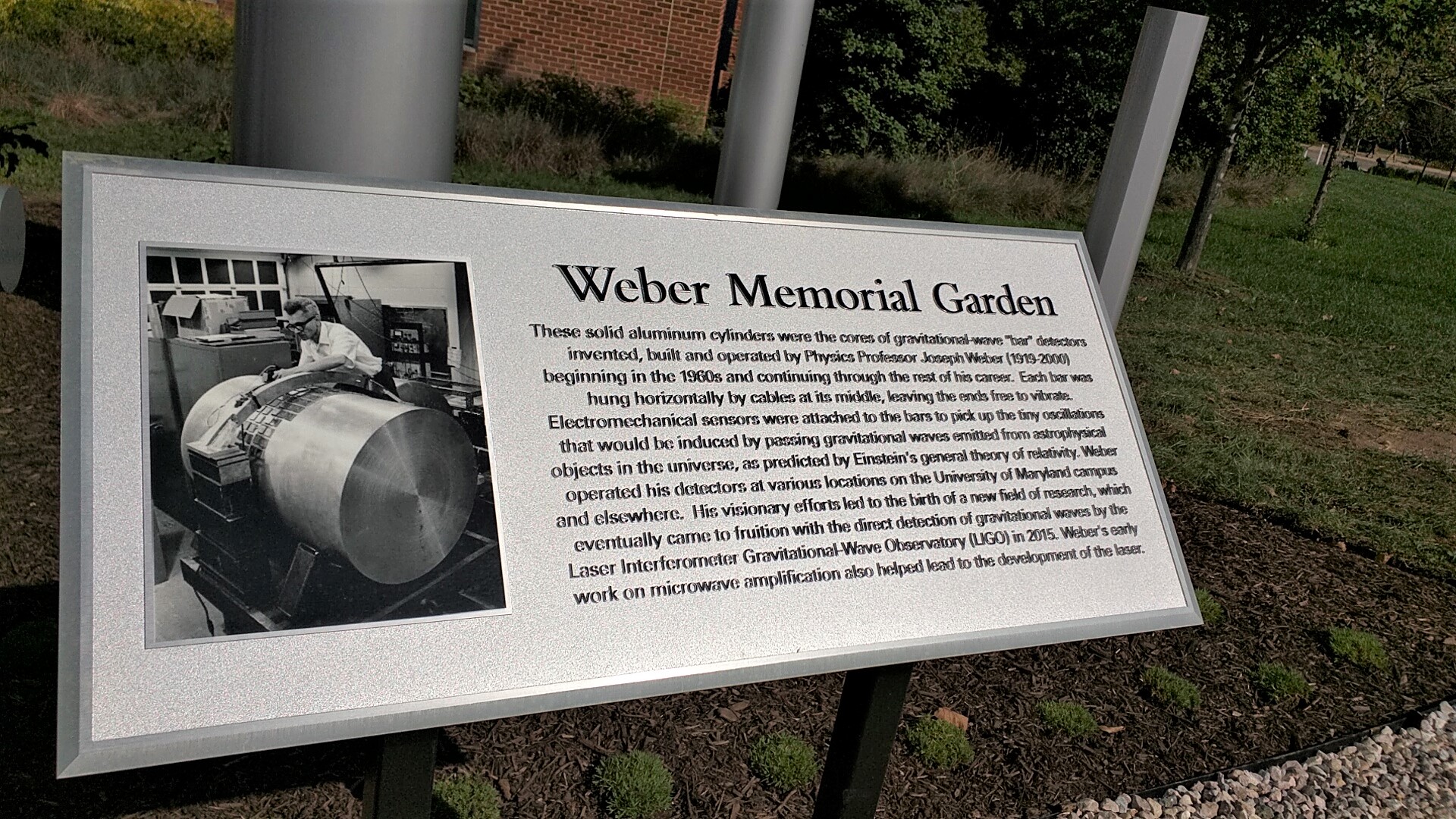
 The Department of Physics and College of Mathematical and Natural Sciences held a dedication of the Weber Garden on Tuesday, March 12, 2019, which included remarks by colleagues and friends of Joe Weber and a colloquium by