Novel Design May Boost Efficiency of On-Chip Frequency Combs
- Details
- Published: Tuesday, October 12 2021 10:46
On the cover of the Pink Floyd album Dark Side of the Moon, a prism splits a ray of light into all the colors of the rainbow. This multicolored medley, which owes its emergence to the fact that light travels as a wave, is almost always hiding in plain sight; a prism simply reveals that it was there. For instance, sunlight is a mixture of many different colors of light, each bobbing up and down with their own characteristic frequency. But taken together the colors merge into a uniform yellowish glow.
A prism, or something like it, can also undo this splitting, mixing a rainbow back into a single beam. Back in the late 1970s, scientists figured out how to generate many colors of light, evenly spaced in frequency, and mix them together—a creation that became known as a frequency comb because of the spiky way the frequencies lined up like the teeth on a comb. They also overlapped the crests of the different frequencies in one spot, making the colors come together to form short pulses of light rather than one continuous beam.
As frequency comb technology developed, scientists realized that they could enable new laboratory developments(link is external), such as ultra-precise optical atomic clocks, and by 2005 frequency combs had earned two scientists a share of the Nobel Prize(link is external) in physics. These days, frequency combs are finding uses in modern technology, by helping self-driving cars to “see” and allowing optical fibers to transmit many channels worth of information at once, among others.
Now, a collaboration of researchers at the University of Maryland (UMD) has proposed a way to make chip-sized frequency combs ten times more efficient by harnessing the power of topology—a field of abstract math that underlies some of the most peculiar behaviors of modern materials. The team, led by Mohammad Hafezi and Kartik Srinivasan, as well as Yanne Chembo, an associate professor of electrical and computer engineering at UMD and a member of the Institute for Research in Electronics and Applied Physics, published their result(link is external) recently in the journal Nature Physics.
“Topology has emerged as a new design principle in optics in the past decade,” says Hafezi, “and it has led to many intriguing new phenomena, some with no electronic counterpart. It would be fascinating if one also finds an application of these ideas.”
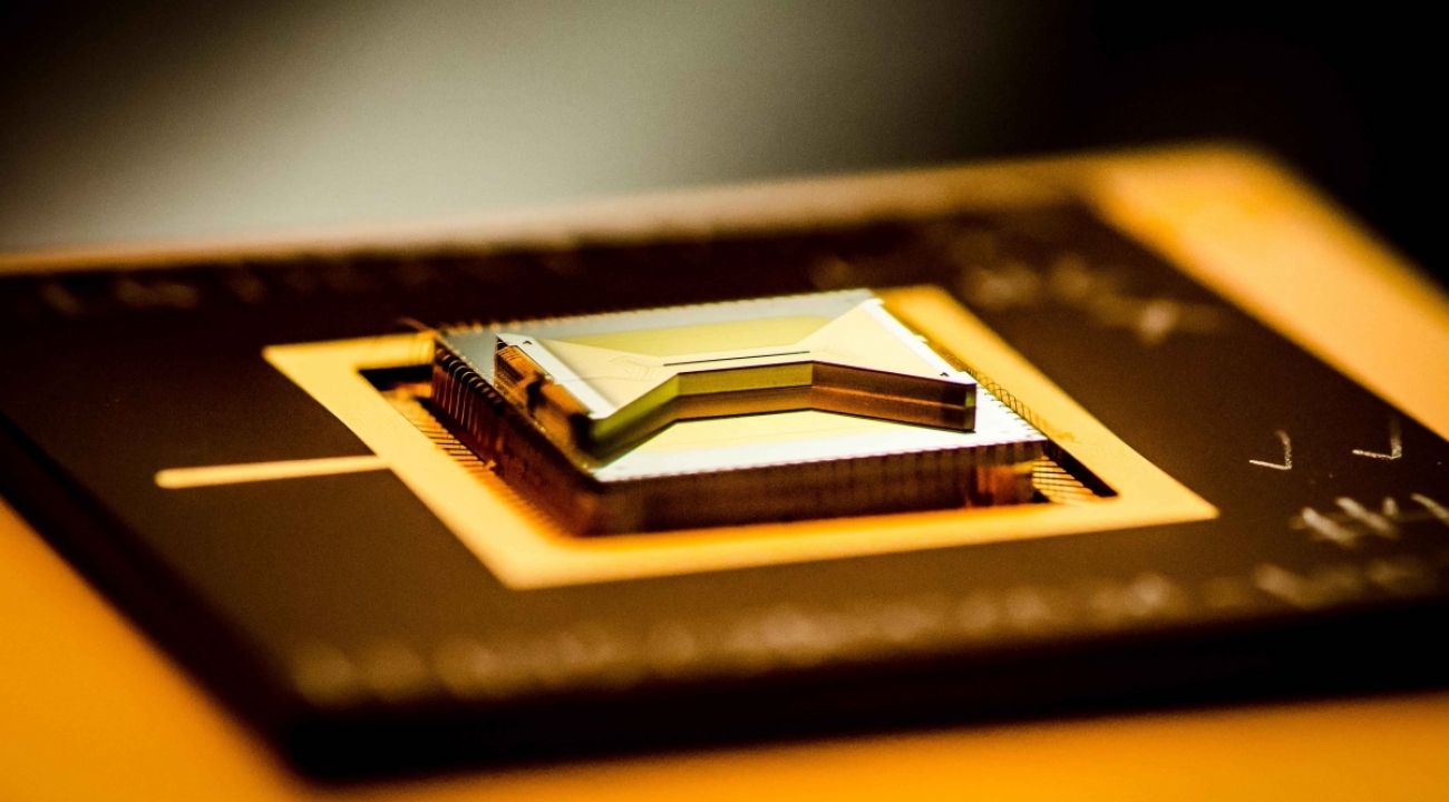
Small chips that can generate a frequency comb have been around for almost fifteen years. They are produced with the help of micro-ring resonators—circles of material that sit atop a chip and guide light around in a loop. These circles are usually made of a silicon compound that is 10 to 100 microns in diameter and printed directly on a circuit board.
Light can be sent into the micro-ring from an adjacent piece of silicon compound, deposited in a straight line nearby. If the frequency of light matches one of the natural frequencies of the resonator, the light will go around and around thousands of times—or resonate—building up the light intensity in the ring before leaking back out into the straight-line trace.
Circling around thousands of times gives the light many chances to interact with the silicon (or other compound) it’s traveling through. This interaction causes other colors of light to pop up, distinct from the color sent into the resonator. Some of those colors will also resonate, going around and around the circle and building up power. These resonant colors are at evenly spaced frequencies—they correspond to wavelengths of light that are an integer fraction of the ring circumference, folding neatly into the circle and forcing the frequencies to form the teeth of a comb. At precisely the right input power and color, the crests of all the colors overlap automatically, making a stable comb. The evenly spaced colors that make up the comb come together to form a single, narrow pulse of light circulating around the ring.
“If you tune the power and the frequency of the light going into the resonator to be just right, magically at the output you get these pulses of light,” says Sunil Mittal, a postdoctoral researcher at the Joint Quantum Institute (JQI) and the lead author of the paper.
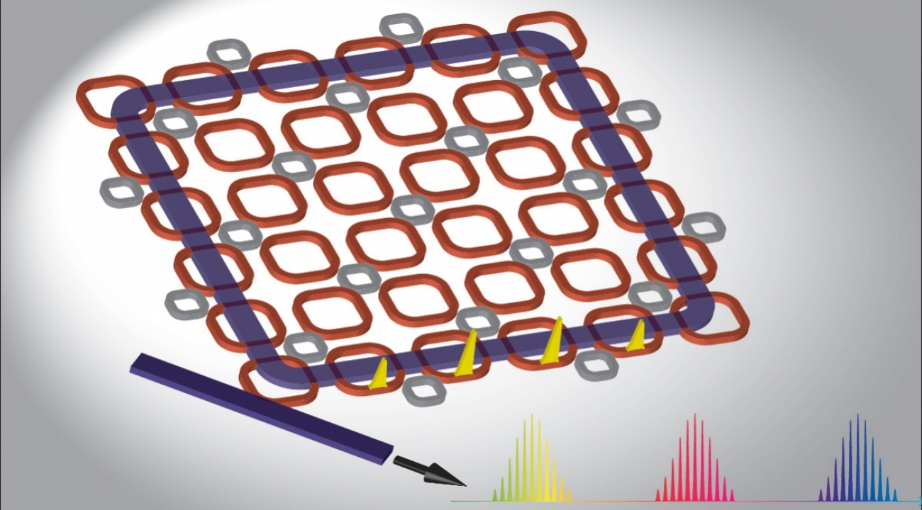
On-chip frequency combs allow for compact app Rendering of a light-guiding lattice of micro-rings that researchers predict will create a highly efficient frequency comb. (Credit: S. Mittal/JQI)lications. For example, light detection and ranging (LIDAR) allows self-driving cars to detect what’s around them by bouncing short pulses of light produced by a frequency comb off its surroundings. When the pulse comes back to the car, it’s compared against another frequency comb to get an accurate map of the surroundings. In telecommunications, combs can be used to transmit more information in one optical fiber by writing different data onto each of the comb teeth using a technique called wavelength-division multiplexing (WDM).
But chip-scale frequency combs also have their limitations. In one micro-ring, the fraction of power that can be converted from the input into a comb at the output—the mode efficiency—is fundamentally limited to only 5%.
Mittal, Hafezi, and their collaborators have previously pioneered a micro-ring array with built-in topological protection, and used it to supply single photons on demand and generate made-to-order entangled photons. They wondered if a similar setup—a square lattice of micro-ring resonators with extra “link” rings—could also be adapted to improve frequency comb technology.
In this setting, the micro-rings along the outer edge of the lattice become distinct from all the rings in the middle. Light sent into the lattice spends most of its time along this outer edge and, due to the nature of the topological constraints, it doesn’t scatter into the center. The researchers call this outer circle of micro-rings a super-ring.
The team hoped to find magic conditions that would form a frequency comb in the pulses circulating around the super-ring. But this is tricky: Each of the rings in the lattice can have its own pulse of light circling round and round. To get one big pulse of light going around the super-ring, the pulses within each micro-ring would have to work together, syncing up to form an overall pulse going around the entire boundary.
Mittal and his collaborators didn’t know at what frequency or power this would happen, or if it would work at all. To figure it out, Mittal wrote computer code to simulate how light would traverse the 12 by 12 ring lattice. To the team’s surprise, not only did they find parameters that made the micro-ring pulses sync up into a super-ring pulse, but they also found that the efficiency was a factor of ten higher than possible for a single ring comb.
With “magic” input color and power, a lattice of micro-rings produces a single pulse of light circulating around the super-ring outer edge. This pulse is made up of equally spaced frequencies forming a highly efficient comb. (Credit: S. Mittal/JQI)
This improvement owes everything to the cooperation between micro-rings. The simulation showed that the comb’s teeth were spaced in accordance with the size of individual micro-rings, or wavelengths that fold neatly around the small circle. But if you zoomed in on any of the individual teeth, you’d see that they were really subdivided into smaller, more finely spaced sub-teeth, corresponding to the size of the super-ring. Simply put, the incoming light was coupled with a few percent efficiency into each of these extra sub-teeth, allowing the aggregate efficiency to top 50%.
The team is working on an experimental demonstration of this topological frequency comb. Using simulations, they were able to single out silicon nitride as a promising material for the micro-rings, as well as figure out what frequency and power of light to send in. They believe constructing their superefficient frequency comb should be within reach of current state-of-the art experimental techniques.
If such a comb is built, it may become important to the future development of several key technologies. The higher efficiency could benefit applications like LIDAR in self-driving cars or compact optical clocks. Additionally, the presence of finely spaced sub-teeth around each individual tooth could, for example, also help add more information channels in a WDM transmitter.
And the team hopes this is just the beginning. “There could be many applications which we don't even know yet,” says Mittal. “We hope that there'll be much more applications and more people will be interested in this approach.”
Original story by Dina Genkina: https://jqi.umd.edu/news/novel-design-may-boost-efficiency-on-chip-frequency-combs


![Schematics of the RC trained for predicting the time series k time steps ahead. Lower: the four time series represent scalar components of X[t]. Schematics of the RC trained for predicting the time series k time steps ahead. Lower: the four time series represent scalar components of X[t].](/images/research_news/neuro1.png)

