A Frankenstein of Order and Chaos

Normally the word “chaos” evokes a lack of order: a hectic day, a teenager’s bedroom, tax season. And the physical understanding of chaos is not far off. It’s something that is extremely difficult to predict, like the weather. Chaos allows a small blip (the flutter of a butterfly wing) to grow into a big consequence (a typhoon halfway across the world), which explains why weather forecasts more than a few days into the future can be unreliable. Individual air molecules, which are constantly bouncing around, are also chaotic—it’s nearly impossible to pin down where any single molecule might be at any given moment.

Now, you might wonder why anyone would care about the precise location of a single air molecule. But you might care about a property shared by a whole bunch of molecules, such as their temperature. Perhaps unintuitively, it is the chaotic nature of the molecules that allows them to fill up a room and reach a single temperature. The individual chaos ultimately gives rise to collective order.

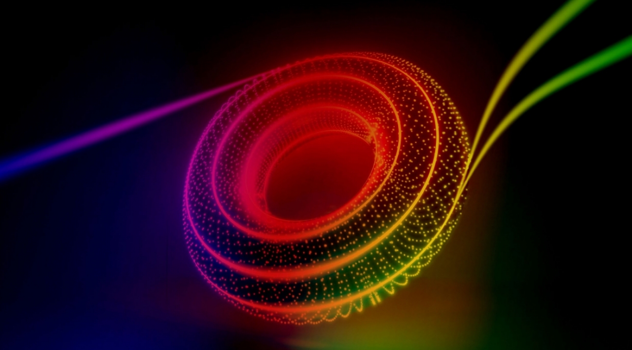
Being able to use a single number (the temperature) to describe a bunch of particles bouncing around in some crazy, unpredictable way is extremely convenient, but it doesn’t always happen. So, a team of theoretical physicists at JQI set out to understand when this description applies.Researchers at JQI have discovered a quantum system that is a hybrid of order and chaos. (Credit: geralt/Pixabay)Researchers at JQI have discovered a quantum system that is a hybrid of order and chaos. (Credit: geralt/Pixabay)

"The ambitious goal here is to understand how chaos and the universal tendency of most physical systems to reach thermal equilibrium arises from fundamental laws of physics," says Victor Galitski, a Fellow of the Joint Quantum Institute (JQI).

As a first step towards this ambitious goal, Galitski and two colleagues set out to understand what happens when many particles, each of which is chaotic on its own, get together. For example, the motion of a single puck in an air hockey game, bouncing uninterrupted off the walls, is chaotic. But what happens when a lot of these pucks are let loose onto the table? And furthermore, what would happen if the pucks obey the rules of quantum physics?

In a paper published recently in the journal Physical Review Letters(link is external), the team studied this air hockey problem in the quantum realm. They discovered that the quantum version of the problem (where pucks are really quantum particles like atoms or electrons) was neither ordered nor chaotic, but a little bit of both, according to one common way of measuring chaos. Their theory was general enough to describe a range of physical settings, including molecules in a container, a game of quantum air hockey, and electrons bouncing around in a disordered metal, such as copper wire in your laptop.

“We always thought it was a problem that’s been solved a long time ago in some textbook,” says Yunxiang Liao, a JQI postdoc and the first author on the paper. “It turns out it's a more difficult problem than we imagined, but the results are also more interesting than we imagined.”

One reason this problem has remained unsolved for so long is that once quantum mechanics enters the picture, the usual definitions of chaos don’t apply. Classically, the butterfly effect—tiny changes in initial conditions causing drastic changes down the line—is often used as a definition. But in quantum mechanics, the very notion of initial or final position doesn’t quite make sense. The uncertainty principle says that the position and speed of a quantum particle can’t be precisely known at the same time. So, the particle’s trajectory isn’t very well defined, making it impossible to track how different initial conditions lead to different outcomes.

One tactic for studying quantum chaos is to take something classically chaotic, like a puck bouncing around an air hockey table, and treat it quantum mechanically. Surely, the classical chaos should translate over. And indeed, it does. But when you put more than one quantum puck in, things become less clear.

Classically, if the pucks can bounce off each other, exchanging energy, they will eventually all reach a single temperature, exposing the collective order of the underlying chaos. But if the pucks don’t bump into each other, and instead pass through each other like ghosts, their energies will never change: the hot ones will stay hot, the cold ones will stay cold, and they’ll never reach the same temperature. Since the pucks don’t interact, collective order can’t emerge from the chaos.

The team took this game of ghost air hockey into the quantum mechanical realm expecting the same behavior—chaos for one quantum particle, but no collective order when there are many. To check this hunch, they picked one of the oldest and most widely used (albeit not the most intuitive) tests of quantum chaos.

Quantum particles can’t just have any energy, the available levels are ‘quantized,’ which basically means they are restricted to particular values. Back in the 1970’s, physicists found that if the quantum particles behaved in predictable ways, their energy levels were completely independent of one another—the possible values didn’t tend to bunch up or spread out, on average. But if the quantum particles were chaotic, the energy levels seemed to avoid each other, spreading out in distinctive ways. This energy level repulsion is now often used as one of the definitions of quantum chaos.

Since their hockey pucks didn’t interact, Liao and her collaborators weren’t expecting them to agree on a temperature, meaning that they wouldn’t see any indications of the underlying single-puck chaos. The energy levels, they thought, would not care about each other at all.

Not only did they find theoretical evidence of some level repulsion, a hallmark of quantum chaos, but they also found that some of the levels tended to bunch together rather than repel, a novel phenomenon that they couldn’t quite explain. This deceptively simple problem turned out to be neither ordered nor chaotic, but some curious combination of the two that hadn’t been seen before.

The team was able to uncover this hybrid using an innovative mathematical approach. “In previous numerical studies, researchers were only able to include 20 or 30 particles,” says Liao. “But using our mathematical approach from random matrix theory, we could include 500 or so. And this approach also allows us to calculate the analytic behavior for a very large system.”

Armed with this mathematical framework, and with piqued interest, the researchers are now extending their calculations to gradually allow the hockey pucks to interact little by little. "Our preliminary results indicate that thermalization may happen via spontaneous breaking of reversibility—the past becomes mathematically distinct from the future,” says Galitski. “We see that small disturbances get exponentially magnified and destroy all remaining signatures of order. But this is another story."

Story by Dina Genkina

In addition to Liao and Galitski, Amit Vikram, a JQI graduate student in physics at UMD, was an author on the paper.

Reference Publication
Research Contact
Victor Galitski This email address is being protected from spambots. You need JavaScript enabled to view it.
(link sends e-mail)
Yunxiang Liao This email address is being protected from spambots. You need JavaScript enabled to view it.
(link sends e-mail)
Original story: https://jqi.umd.edu/news/frankenstein-order-and-chaos

Enhanced Frequency Doubling Adds to Photonics Toolkit

The digital age has seen electronics, including computer chips, shrink in size at an amazing rate, with ever tinier chips powering devices like smartphones, laptops and even autonomous drones. In the wake of this progress, another miniature technology has been gaining steam: integrated photonics.

Photons, which are the quantum particles of light, have some advantages over electrons, the namesakes of electronics. For some applications, photons offer faster and more accurate information transfer and use less power than electrons. And because on-chip photonics are largely built using the same technology created for the electronics industry, they carry the promise of integrating electronics and photonics on the same chip.

Tiny photonic chips have already been adopted in many places, including telecommunications networks (think fiber optic internet) and large data centers (think interfacing fiber-optics with electronics). Other industries are on the precipice of benefitting from photonics, with self-driving car makers developing(link is external) light-based radar chips. However, many tools that are well-established in traditional optics—things that use lasers, lenses and other bulky equipment—do not yet have a compact photonic analogue. For futuristic tools like light-based quantum computers or portable optical clocks, more work remains to package everything together.

Now, researchers at the Joint Quantum Institute (JQI) have added a new tool to the photonics toolkit: a way to use silicon, the native material for much of digital electronics and photonics, to efficiently double the frequency of laser light. By combining two existing techniques, the team achieved a frequency doubling efficiency 100 times greater than previously experiments with silicon compounds. They detailed their results in a paper published in the journal Nature Photonics(link is external).

Light waves are made up of photons, but they also carry a frequency. Our eyes see a small fraction of these frequencies as the colors of the rainbow, but microwaves, x-rays and radio waves (among others) also inhabit this spectrum. Doubling the frequency of light is one way to convert between these different ranges. In the new work, the team demonstrated a doubling of infrared light—commonly used in optical telecommunications—to red light, the language of very precise atomic clocks.

Frequency doubling is one effect that can occur when light interacts with the medium it’s traveling through, be it air, water or silicon. Depending on the properties of these materials, a little bit of the light can be doubled, tripled, or, in extreme cases, multiplied to even higher degrees, like a musical note also generating a bit of sound one, two, or several octaves up. By choosing the right material, and illuminating it in the right way, researchers can get to the harmonic they need.

Unfortunately, silicon and silicon compounds—the materials of choice for routing light on a chip because of the maturity of silicon manufacturing and the ease of integrating with elA new photonic chip can double the frequency (f) of incoming light using a circular ring 23 microns across. The ring is tailored to generate and hold light at the input frequency and at its second harmonic (2f)—just like piano strings or organ tubes can host harmonics of a single tone. The color indicates crests and troughs of the light field, similar to a piano string’s displacement pattern when it rings. (Credit: Xiyuan Lu/NIST and UMD)A new photonic chip can double the frequency (f) of incoming light using a circular ring 23 microns across. The ring is tailored to generate and hold light at the input frequency and at its second harmonic (2f)—just like piano strings or organ tubes can host harmonics of a single tone. The color indicates crests and troughs of the light field, similar to a piano string’s displacement pattern when it rings. (Credit: Xiyuan Lu/NIST and UMD)ectronics—don’t intrinsically support frequency doubling. The crystal structure is too uniform, meaning it looks the same in all directions. This prohibits the doubling effect, which relies on electrons in the material shifting one way more than another under the influence of light. But once light is confined to a tiny trace on a chip, things become a little less uniform: After all, the air is always nearby, and it doesn’t look at all like a silicon crystal. So, a tiny amount of frequency doubled light does get generated, but usually it is not enough to be useful.

In the new work, a team led by Adjunct Professor Kartik Srinivasan, a Fellow of the National Institute of Standards and Technology (NIST), and NIST and UMD postdoctoral researcher Xiyuan Lu, combined two previously explored techniques to build on this tiny effect, generating 100 times more frequency doubled light than any previous silicon experiments. Additionally, their doubling occurred with an efficiency of 22%, appreciable enough to be useful in applications.

The first trick was to capture the light in a resonator, making the light go round and round and triggering the tiny doubling effect over and over again. To achieve this, the researchers first routed near-infrared laser light into an optical fiber. The fiber then shot the light into a silicon nitride waveguide printed on a silicon chip. This waveguide led to another waveguide, which was wrapped into a circle just 23 microns in diameter. The circular resonator, which was engineered to capture the incoming light and circulate it around, allowed a tiny bit of frequency doubling to happen over and over again. Another straight waveguide, on the other edge of the resonator, was tuned to carry away the frequency-doubled light.

The second trick was to make the silicon less uniform by biasing it with an electric field. Luckily, no external field was actually needed—the tiny amount of frequency doubled light, combined with the original infrared pump light, caused the electrons in the resonator to gather at the edges, creating a constant electric field. This field greatly enhanced the frequency doubling capacity of the silicon nitride.

“It’s a feedback process,” says Srinivasan, “because a little bit of frequency doubled light and pump light start to create the constant electric field, making the frequency doubling process stronger, which in turn creates more frequency doubled light. So both the pump light and the frequency doubled light are circulating around in this ring, and there’s this huge ability to take this thing that started out as extremely weak, and then actually make it a pretty strong effect.”

Getting both of these effects to work in the same device wasn’t easy. Not only does the resonator ring need to be exactly the right size to trap the pump and frequency doubled light, the light also needs to stack up in the right way in the resonator. To achieve this, detailed simulations and precise manufacturing in a clean room are necessary. But once such an accurate device is fabricated, all you need to do is send in pump light, and observe frequency doubled light at the output.

“To enable efficient interaction between light and the material, light of different colors has to live a long time and also move at exactly the same speed,” says Lu, “Our device implements these two key factors into photo-induced frequency doubling, which significantly boosts the power efficiency of this process.”

This device is another step in a long quest to achieve a portable, ultra-precise atomic clock. “These optical clocks are these amazing timekeeping devices, but usually they're in a big lab,” says Srinivasan. “If it could be in a small package it could go on cars or drones or other vehicles. Timing underlies a lot of important navigation applications, and for the most part, now, people rely upon GPS signals. But there are all sorts of possibilities that there might be something in the way, and you can’t acquire those signals, or somebody spoofs the signal. So, having portable timing instruments that could really give you accurate and precise time for long stretches before you need a synchronization signal from GPS is meaningful.”

Although it’s not the star of the show, frequency doubling is a necessary component in optical atomic clocks. These clocks produce an extremely regular beat, but at optical frequencies—hundreds of trillions of light field oscillations per second. Conventional electronics can’t interface with that signal directly, so to bring this precision down to an intelligible frequency (mere billions of oscillations per second) scientists use frequency combs—laser sources with frequency ‘teeth’ at perfectly regular intervals, an invention that won the 2005 Nobel Prize in physics(link is external).

To be useful, these frequency combs need to be calibrated—each tooth in the comb needs to be labeled with a specific frequency value. The simplest and most common way to calibrate them is to take the lowest tooth in the comb, frequency double it, and compare to the highest tooth: this gives the frequency of the lowest tooth. Along with a simple measurement of the spacing between teeth, scientists can use this to deduce the exact frequency of each tooth.

Recently, several pieces of the on-chip atomic clocks, including tiny atomic vapor cells and on-chip frequency combs, have been achieved in silicon-based photonics. However, the frequency doubling calibration was previously done with bulky optics or using materials that are less compatible with silicon. “At least conceptually,” says Srinivasan, “we’re one step closer to a calibrated frequency comb in a really compact package. There's still work to be done to really be able to put these things together, but we’re closer to a compact optical atomic clock than we were before.”

Original story by Dina Genkina: https://jqi.umd.edu/news/enhanced-frequency-doubling-adds-photonics-toolkit

In addition to Srinivasan and Lu, this paper had 3 additional co-authors: Gregory Moille, a postdoctoral researcher at JQI and NIST; Ashutosh Rao, a postdoctoral researcher in chemistry and biochemistry at UMD and NIST; and Daron A. Westly, a research scientist at NIST

Research Contact: Kartik Srinivasan (This email address is being protected from spambots. You need JavaScript enabled to view it.)

UMD-NIST Self-Directing AI System Discovers New Material

When the words “artificial intelligence” (AI) come to mind, your first thoughts may be supercomputers, or robots that perform tasks without assistance from humans. Now, a multi-institutional team led by researchers from the University of Maryland (UMD) and National Institute of Standards and Technology (NIST) working with collaborators at Stanford University, University of Washington, University of Pennsylvania, and Duke University have accomplished something not too far off. They developed an AI algorithm called CAMEO that discovered a useful new material without requiring additional training from scientists. The AI system could help reduce the amount of trial-and-error time scientists spend in the lab, while maximizing productivity and efficiency in their research.

The research team published their work on CAMEO in Nature Communications on November 24, 2020.

In the field of materials science, scientists seek to discover new materials that can be used in specific applications. “For example, we are always looking are new quantum materials which can be used for quantum computers and sensors,” said physics affiliate Ichiro Takeuchi, a professor of materials science and engineering and member of the Quantum Materials Center (QMC) at UMD.

But finding such new materials usually takes a large number of coordinated experiments and time-consuming theoretical searches. If a researcher is interested in how a material’s properties vary with different temperatures, then that may mean 10 experiments at 10 different temperatures. Temperature, however, is just one parameter. If there are five parameters, each with 10 values, then that researcher must run the experiment 10 x 10 x 10 x 10 x 10 times, a total of 100,000 experiments. It’s nearly impossible for a researcher to run that many experiments via brute force due to the years or decades it may take.

That’s where CAMEO comes in. Short for Closed-Loop Autonomous System for Materials Exploration and Optimization, CAMEO can ensure that each experiment maximizes the scientist’s knowledge and understanding, skipping over experiments that would give redundant information. Helping scientists reach their goals faster with fewer experiments also enables  labs to use their limited resources more efficiently. But how is CAMEO able to do this?

Method Behind the Process

Active learning is a machine learning technique in which computer programs can access data and process it themselves, automatically updating the knowledge and deciding the optimum sequence of information acquisition. This is the basis for CAMEO, a self-learning AI that uses prediction and uncertainty to determine which experiment to try next.

As implied by its name, CAMEO looks for a useful new material by operating in a closed loop: it determines which experiment to run on a material, does the experiment, and collects the data. It can also ask for more information, such as the crystal structure of the desired material, from the scientist before running the next experiment, which is informed by all past experiments achieved in the loop.  

“The key to our experiment was that we were able to unleash CAMEO on a combinatorial library where we had made a large array of materials with all different compositions,” said Takeuchi. “In a usual combinatorial study, every material in the array would have been measured one by one to look for the compound with the best properties. Depending on the property of interest, even with a fast measurement setup, that can take a long, long time. With CAMEO, it only took a small fraction of total number of measurements to home in on the best material.”

The AI is also designed to contain knowledge of key principles, some of which includes knowledge of past simulations and lab experiments, how the equipment works, and physical concepts. For example, the researchers armed CAMEO with the knowledge of phase diagrams, which describes how the arrangement of atoms in a material changes with chemical composition and temperature.

Understanding how atoms are arranged in a material is important in determining its properties such as how hard, or how electrically-insulating it is, and how well it is suited for a specific application.

“The AI is unsupervised,” said NIST researcher, Aaron Gilad Kusne. “Many types of AI need to be trained or supervised. Instead of asking it to learn physical laws, we encode them into the AI. You don’t need a human to train the AI.”

One of the best ways to figure out the structure of a material is by bombarding it with x-rays, in a technique called x-ray diffraction. By identifying the angles at which the x-rays bounce off, scientists determine how atoms are arranged in a material, enabling them to figure out its crystal structure. However, a single in-house x-ray diffraction experiment can take an hour or more. At a synchrotron facility, a large machine the size of a football field that accelerates electrically charged particles at close to the speed of light, this process can take 10 seconds, because the fast-moving particles emit large numbers of x-rays. This is the method used in the study at the Stanford Synchrotron Radiation Lightsource.

CAMEO then decides which material composition to study next and focuses the x-rays on the appropriate part of the sample where that composition exists, to investigate its atomic structure. With each new iteration, CAMEO learns from past measurements and identifies the next material to study.  This allows the AI to explore how a material’s composition impacts its structure and use this information to find the best material for the task.

“Think of this process as trying to make the perfect cake,” Kusne said. “You’re mixing different types of ingredients, flour, eggs, or butter, using a variety of recipes to make the best cake. With the AI, it’s searching through the ‘recipes’ or experiments to determine the best composition for the material.”

That is how CAMEO discovered the material  which the group shortened to GST467. CAMEO was provided with 177 potential materials to investigate, covering a large range of compositional recipes. To arrive at this material, CAMEO performed 19 different experimental cycles, which took 10 hours, compared to the estimated 90 hours it would have taken a scientist with the full set of 177 materials.

The New Material

The material is composed of three different elements (germanium, antimony and tellurium, Ge-Sb-Te) and is a phase-change memory material, that is, it changes its atomic structure from crystalline (solid material with atoms in designated, regular positions) to amorphous (solid material with atoms in random positions) when quickly melted by applying heat. This type of material is used in memory applications such as data storage. Although there are infinite composition variations possible in the Ge-Sb-Te alloy system, the new material GST467 discovered by CAMEO is optimal for phase-change applications.

The research team wanted CAMEO to find the best Ge-Sb-Te alloy, one that had the largest difference in optical contrast between the crystalline and amorphous states. Optical contrast, for example on a DVD disc, allows a scanning laser to read the disc by distinguishing between regions that have high or low reflectivity. They found that GST467 has twice the contrast for a phase change material compared to GST225 or , a well-known material that’s commonly used for DVDs. The larger contrast enables the new material to outperform the old material by a significant margin.

The key part of the experiments was conducted at the Stanford National Accelerator Laboratory (SLAC) at Stanford University, for the U.S. Department of Energy Office of Science. SLAC researchers helped oversee the experiments run by CAMEO.

UMD researchers provided the materials used in the experiments and researchers at the University of Washington – led by Electrical and Computer Engineering Professor, Mo Li – demonstrated the new material in a patterned phase-change memory device. 

The new material GST467 has applications for photonic switching devices, which control the direction of light in a circuit. They can also be applied in neuromorphic computing, a field of study focused on developing devices that emulate the structure and function of neurons in the brain, opening possibilities for new kinds of computers as well as other applications such as extracting useful data from complex images.

The work also involved collaboration with electron microscopists at NIST who performed high-resolution microscopy to understand the microstructure of the newly found compound.

Applications to other Materials

The researchers believe CAMEO can be used for other types of materials, such as high-temperature alloys and quantum materials. The code for CAMEO is open source and will be freely available for use by scientists and researchers.

There had been other reports of closed-loop materials and chemistry optimization work. The critical distinguishing feature of the present work with CAMEO is that it was used to discover a novel solid state material whose functionality is encoded in the composition-structure-property relationship of crystalline materials, and as such, the algorithm was able to navigate the course of discovery path by tracking the structural origins of materials functionalities.

One application of CAMEO is minimizing experimental costs since using synchrotron facilities requires time, researchers need a written proposal to use the equipment, and money. But with AI running the experiments, they can be carried out quicker. Researchers estimate a 10-fold reduction in time for experiments using CAMEO since the number of experiments performed can be cut by one tenth. Because the AI is running the measurements, collecting data and performing the  analysis, this also reduces the amount of knowledge a researcher needs to run the experiment. All the researcher must focus on is running the AI.

Another potential benefit is providing the ability to work remotely for scientists. “This opens up a wave of scientists to still work and be productive without actually being in the lab,” said SLAC researcher Apurva Mehta. This could mean if scientists wanted to work on research involving contagious diseases or viruses, such as COVID-19, they could do so safely and remotely while relying on the AI to conduct the experiments in the lab.

Researchers are continuing to improve the AI and try to make the algorithms capable of solving ever more complex problems. “The ultimate goal is to incorporate synthesis of crystalline materials in the closed loop – this is particularly hard since standard synthesis tools of crystalline functional materials are not equipped with measurement capabilities,” said Takeuchi. “That calls for some novel hardware integration as well as advances in AI. The future is robot materials science.”  

Original story: https://mse.umd.edu/news/story/umdnist-selfdirecting-ai-system-discovers-new-material

Going Beyond the Anti-Laser May Enable Long-Range Wireless Power Transfer

Ever since Nikola Tesla spewed electricity out in all directions with his coil back in 1891, scientists have been thinking up ways to send electrical power through the air. The dream is to charge your phone or laptop, or maybe even a healthcare device such as a pacemaker, without the need for wires and plugs. The tricky bit is getting the electricity to find its intended target, and getting that target to absorb the electricity instead of just reflect it back into the air—all preferably without endangering anyone along the way.

These days, you can wirelessly charge a smartphone by putting it within an inch of a charging station. But usable long-range wireless power transfer, from one side of a room to another or even across a building, is still a work in progress. Most of the methods currently in development involve focusing narrow beams of energy and aiming them at their intended target. These methods have had some success, but are so far not very efficient. And having focused electromagnetic beams flying around through the air is unsettling.Arcs of electricity generated by a Tesla coil. (Credit: Airarcs/CC BY-SA 3.0)Arcs of electricity generated by a Tesla coil. (Credit: Airarcs/CC BY-SA 3.0)

Now, a team of researchers at the University of Maryland (UMD), in collaboration with a colleague at Wesleyan University in Connecticut, have developed an improved technique for wireless power transfer technology that may promise long-range power transmission without narrowly focused and directed energy beams. Their results, which widen the applicability of previous techniques, were published Nov. 17, 2020 in the journal Nature Communications.

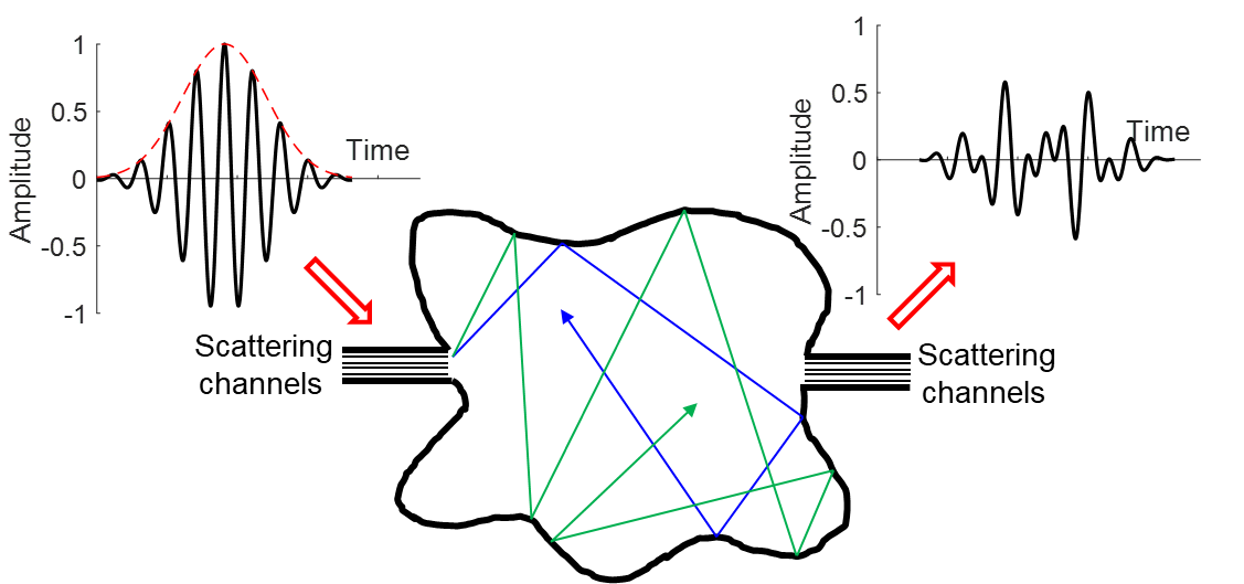
The team generalized a concept known as an “anti-laser.” In a laser, one photon triggers a cascade of many photons of the same color shooting out in a coherent beam. In an anti-laser, the reverse happens. Instead of boosting the number of photons, an anti-laser coherently and perfectly absorbs a beam of many precisely tuned photons. It’s kind of like a laser running backwards in time.

The new work, led by UMD Professor of Physics Steven Anlage of the Quantum Materials Center (QMC), demonstrates that it’s possible to design a coherent perfect absorber outside of the original time-reversed laser framework—a relaxation of some of the key constraints in earlier work. Instead of assuming directed beams traveling along straight lines into an absorption target, they picked a geometry that was disorderly and not amenable to being run backwards in time.

“We wanted to see this effect in a completely general environment where there's no constraints,” says Anlage. “We wanted a sort of random, arbitrary, complex environment, and we wanted to make perfect absorption happen under those really demanding circumstances. That was the motivation for this, and we did it.”

Anlage and his colleagues wanted to create a device that could receive energy from a more diffuse source, something that was less beam and more bath. Before tackling the wireless challenge, they set up their generalized anti-laser as a labyrinth of wires for electromagnetic waves to travel through. Specifically, they used microwaves, a common candidate for power transfer applications. The labyrinth consisted of a bunch of wires and boxes connected in a purposefully disordered way. Microwaves going through this labyrinth would get so tangled up that, even if it were possible to reverse time, this still wouldn’t untangle them.

Buried in the midst of this labyrinth was an absorber, the target to deliver power to. The team sent microwaves of different frequencies, amplitudes and phases into the labyrinth and measured how they were transformed. Based on these measurements, they were able to calculate the exact properties of input microwaves that would result in perfect power transfer to the absorber. They found that for correctly chosen input microwaves, the labyrinth absorbed an unprecedented 99.999% of the power they sent into it. This showed explicitly that coherent perfect absorption can be achieved even without a laser run backwards in time.

The team then took a step towards wireless power transfer. They repeated the experiment in a cavity, a plate of brass several feet in each direction with an oddly shaped hole in the middle. The shape of the hole was designed so that the microwaves would bounce around it in an unpredictable, chaotic way. They placed a power absorber inside the cavity, and sent microwaves in to bounce around the open space inside. They were able to find the right input microwave conditions for coherent perfect absorption with 99.996% efficiency.

Recent work by a collaboration of teams in France and Austria also demonstrated coherent perfect absorption in their own disordered microwave labyrinth. However, their experiment was not quite as general as the new work from Anlage and colleagues. In the previous work, the microwaves entering the labyrinth would still be untangled by a hypothetical reversal of time. This might seem like a subtle distinction, but the authors say showing that coherent perfect absorption doesn’t require any kind of order in the environment promises applicability virtually anywhere.

Generalizing previous techniques in this way invites ideas that sound like science fiction, like being able to wirelessly and remotely charge any object in a complex environment, such as an office building, with near perfect efficiency. Such schemes would require that the frequency, amplitude, and phase of the electric power is custom tuned to specific targets. But there would be no need to focus a high-powered beam and aim it at the laptop or phone—the electrical waves themselves would be designed to find their chosen target.

“If we have an object which we want to deliver power to, we will first use our equipment to measure some properties of the system,” says Lei Chen, a graduate student in electrical and computer engineering at UMD and the lead author of the paper. “Based on those properties we can get the unique microwave signals for this kind of system. And it will be perfectly absorbed by the object. For every unique object, the signals will be different and specially designed.”

Although this technique shows great promise, much remains to be done before the advent of wireless and plug-less offices. The perfect absorber depends crucially on the power being tuned just right for the absorber. A slight change in the environment—such as moving the target laptop or raising the blinds in the room—would require an immediate retuning of all the parameters. So, there would need to be a way to quickly and efficiently find the right conditions for perfect absorption on the fly, without using too much power or bandwidth. Additionally, more work needs to be done to determine the efficacy and safety of this technique in realistic environments.

Even though it’s not yet time to throw away all your power cords, coherent perfect absorption may come in handy in many ways. Not only is it general to any kind of target, it is also not limited to optics or microwaves.  “It's not wedded to one specific technology,” says Anlage, “This is a very general wave phenomenon. And the fact that it's done in microwaves is just because that's where the strengths are in my lab. But you could do all of this with acoustics, you could do this with matter waves, you could do this with cold atoms. You could do this in many, many different contexts.”

In addition to Chen and Anlage, Tsampikos Kottos, a professor at Wesleyan University, was a co-author on the paper.

Written by Dina Genkina (This email address is being protected from spambots. You need JavaScript enabled to view it.)


UMD Physicists Contribute to New B Meson Finding

Scientists have known for decades of a massive imbalance between the amount of matter and antimatter in the universe. To resolve the discrepancy, they attempt to recreate the first instant after the Big Bang through fierce collisions of subatomic particles, followed by intense scrutiny of the resulting forces and pieces.  A premiere effort is CERN’s LHCb experiment, in which B mesons’ disintegration provides clues that may someday explain why matter has predominated over antimatter. Although the Standard Model is shown to contain a mechanism that violates the charge-parity (CP) symmetry – the symmetry that ensures equal treatment of reactions involving matter or antimatter particles – it can only account for a small part of the observed matter-antimatter imbalance in the universe. A major goal of the LHCb experiment is to discover possible sources of CP violation beyond the Standard Model.

Now, the LHCb collaboration has announced a major new development, based on data collected during LHC Run 2, confirming and significantly strengthening an anomalous observation in decays of B mesons. At an October 28 CERN workshop, a result of a measurement of the CP violation in a B meson B+→K+π0 was announced.  This is the most precise measurement of CP asymmetry yet found in this decay, and an important data point in studies of B meson decays, following results gained by the BaBar, Belle and Tevatron experiments, as well as LHCb.  This result significantly strengthens the anomalous difference with the measured CP asymmetry in the counterpart decay channel of the neutral B meson (B0→K+π-), an effect yet to be satisfactorily explained in the Standard Model.The images above show the reconstructed invariant mass distribution of K+π0 and K-π0 mass distributions. Clear enhancements at the B+ (left) and B- (right) masses are visible.The images above show the reconstructed invariant mass distribution of K+π0 and K-π0 mass distributions. Clear enhancements at the B+ (left) and B- (right) masses are visible.

UMD postdoc Will Parker made the recent presentation, which can be seen here.

The UMD flavor physics group has been working on B meson decays since 1995 with the design and development of the BaBar experiment at SLAC and since 2014 with the LHCb experiment at CERN. “We are happy that we now have the most precise measurement of this anomaly, which is of huge interest in the particle physics community,” said Distinguished University Professor Hassan Jawahery.

Along with Jawahery, Parker, Phoebe Hamilton and Jason Andrews (PhD 2018),  who carried out this measurement, the UMD LHCb group includes Assistant Professor Manuel Franco Sevilla, researcher Svende Braun, and graduate students Alex Fernez, Yipeng Sun, and Zishuo Yang. In 2019, the LHCb experiment observed CP violation in decays of D mesons. That finding was rated a Physics World Breakthrough of the Year finalist for 2019

To learn more about the new B+→K+π0 result, see the LHCb announcement: https://lhcb-public.web.cern.ch/Welcome.html#Kpi.  The full paper will be submitted to Physical Review Letters.