Pushing the Frontier of Extreme Light-Matter Interaction Research

University of Maryland Physics Professor Howard Milchberg and the students and postdoctoral researchers in his lab explore the dramatic results of experiments that push light to extremes in the presence of matter. In Milchberg’s opinion, researching the intense interactions between light and matter—which are only possible thanks to the revolutionary technology of lasers—brings together the most interesting aspects of physics.

“Once you considered the effect that an intense laser beam has on matter, the number of basic physics and application areas exploded,” said Milchberg, who also holds appointments in the Department of Electrical and Computer Engineering and the Institute for Research in Electronics and Applied Physics. “And understanding the interaction between intense light and matter requires bringing in tools from all areas of physics. It flexes all your physics muscles, experimental and theoretical, and it overlaps with all of the major areas. You have to deal with atomic physics, plasma physics, condensed matter physics, high-pressure physics and quantum physics. It is intellectually challenging and, as a bonus, it has many practical applications.”

In explorinIntense Laser-Matter Interactions Lab, University of MarylandIntense Laser-Matter Interactions Lab, University of Marylandg this research topic, his lab has discovered new physics and technological opportunities. From cutting-edge, powerful laser pulses to vortices made of light, recent research from Milchberg’s lab keeps revealing new ways that light and matter can come together and deliver new results.

The richness of this line of research comes from the fact that light is much more than just illumination traveling in straight lines at a constant speed. It is energy that can dance intricately as it travels and can interact with matter in exotic ways—including tearing atoms into pieces.

Light is traveling electric and magnetic energy, and it is often convenient to visualize light as traveling waves in the electric and magnetic fields. The hills and troughs in the waves represent the shifting of the strength and direction of the fields that push and pull on charged particles, like the protons and electrons that make up atoms. Powerful lasers can even accelerate charged particles to near the speed of light where the unusual behaviors described by Einstein’s theory of relativity come into play.

Milchberg’s lab often investigates the dramatic results of dialing a laser up to extreme strengths where it exceeds the field that connects the cores of atoms to its electrons. As researchers like Milchberg push lasers to greater and greater power levels, they reach a roadblock: A laser tends to spread its power out over an increasing area as it travels, and a laser with enough power will vaporize any solid piece of equipment that researchers try to use to corral it.

So an optical fiber, like those that commonly carry internet signals, are useless when faced with a powerful research laser. The central core and outer cladding that make up the fiber get destroyed without any chance to keep the light concentrated as it blazes forward.

But Milchberg’s research has uncovered multiple ways to use the interactions of light with matter to keep powerful laser beams contained. In papers published in the journals Physical Review Letters and Physical Review Research over the past year, Milchberg and his colleagues described two new ways to keep intense laser beams contained in a way that can accelerate particles and produce advanced coherent light sources. In addition to improving our understanding of how light and matter interact, the techniques might be implemented as tools for research in other areas, like high-energy physics, and for use in industrial and medical settings.Researchers have generated vortices of light that they describe as “edge-first flying donuts” and developed a new technique for imaging them in mid-flight. (Credit: Scott Hancock/University of Maryland) Researchers have generated vortices of light that they describe as “edge-first flying donuts” and developed a new technique for imaging them in mid-flight. (Credit: Scott Hancock/University of Maryland)

In these projects, the group used its expertise to give the technology of optical fibers an extreme indestructible makeover. The key lies in building the waveguides—devices such as optical fibers that transport waves down a confined path—out of a material that has already been vaporized. The team forms the material—an energetic state of matter called a plasma—by letting a laser rip electrons free from their atoms to form a cloud of charged particles.

“A plasma waveguide has all the structure of an optical fiber, the classic core, the classic cladding,” Milchberg said. “Although in this case, it's indestructible. The hydrogen plasma forming the waveguide is already ripped up into its protons and electrons, so there's not much more violence you can do to it.”

For the first project, the group used two laser pulses: a solid beam and then a hollow tube of light matching the desired form of the outer shell. These two lasers allowed the team to independently craft the low-density cores and outer shells more carefully than previous approaches. This refined control improved the amount of power the techniques could concentrate and the distance the powerful pulses could travel­­­­­—a key to achieving desired levels of acceleration with a compact system.

The second approach produced a similar plasma waveguide but sacrificed the ability to tailor the resulting waveguide in favor of using a simpler, more accessible technique. In this technique, the researchers created a tube of low-density gas and then relied on the front edge of the powerful pulse to rip the electrons free and create the waveguide structure on-the-fly.

“It's actually simpler than the first method,” Milchberg said. “But there's less control. And we did an analysis which shows that if you want to have big diameter waveguides, the first method is actually more efficient than the second method.”

Both methods have potential uses as laser accelerators that can generate bursts of electrons of energy 10 billion electron volts, and Milchberg’s group is already doing those experiments.

In addition to these two techniques, Milchberg’s group is developing a technique that uses a 1,000 times higher density hydrogen gas to accelerate electrons without constructing a waveguide, while using 1,000 times less laser energy. This new technique improves on established methods by avoiding negative effects from the light vibrating the electrons as they get accelerated behind the intense laser pulse.

To do this, they used pulses of circularly polarized light that aren’t even as long as two full lengths of the waves of the light that is used. The field of circularly polarized light rotates as the light travels and this variation cancels out the effect of the asymmetries of the vibration from the light waves, enabling electron beams of higher quality than previous attempts. The denser gas used in this approach isn’t compatible with the 10 billion electron volt energies of the other approaches, but the technique might have its own niche to fill.

“Our experiments have spanned the higher through lower energy ends of laser-based acceleration,” Milchberg said. “The plasma waveguide effort is aimed at 10 billion electron volts, which is of high energy physics interest, while the newer research using millijoule pulses and dense hydrogen generates 15 million electron volts.  Although a high energy, it isn’t enough for high energy physics. But the energy is more than sufficient to do time-resolved medical imaging and materials imaging.”

But accelerating particles is not the only aspect of light-matter interactions that Milchberg’s group investigates. For instance, they also discovered new intricate effects that can be created in light pulses.

In a paper published in the journal Optica in December 2019, they generated and observed a new kind of light structure called a spatiotemporal optical vortex (STOV). STOVs are whorls in the way the phase—the property of light and other waves that tells you are where you are on the wave—changes in space and time. The researchers had to first develop a method to create these vortices and then figure out how to observe them in flight. The observation required analysis of the interaction between the STOVs and another bit of light while traveling through a thin glass window.

Understanding STOVs provides insight into how light produces the high-intensity laser effect called self-guiding. Milchberg’s team had previously discovered a naturally occurring form of STOV that behave like “optical smoke rings” and are crucial for all self-guiding processes. These vortices may also have applications in transmitting information because the twisting structure tends to stabilize itself by filling any sections that get knocked out—say by water droplets in the air that the signal travels through.

All of these research results represent new techniques that may be useful tools for researchers and industry, and they deepen our understanding of the intricate back-and-forth that can be engineered between light and matter.

“One of the things that I would say my group is known for is that all of our papers include theory and simulation that accompanies the experiments,” Milchberg said. “And that has provided an important feedback loop to guide and refine the experiments.”

Milchberg credits his group’s steady generation of new discoveries to his graduate students.

“I don't think I could have done any of this in a non-university setting,” Milchberg said. “I think the sort of relationship one has with students and they have with each other where we're all batting ideas back-and-forth and having a continuous free-for-all discussion—with crazy thoughts encouraged—is not the same as in a place filled with longtime Ph.D.s and an established hierarchy. The freedom to ask naïve questions and argue a lot is essential.”

Written by Bailey Bedford

Researchers Create On-Demand Cold Spots to Generate Electromagnetic Cone of Silence

In modern society, we are accustomed to having electronic systems that always work, regardless of the conditions. Protection of sensitive electronics to interference through unwanted coupling between components or intentional electromagnetic attack is important to ensure uninterrupted service. However, the environments in which we operate are growing increasingly complex and the electromagnetic spectrum is more congested. Additionally, certain environments such as a passenger cabin on an aircraft or train, can act as reverberant cavities, resulting in random fluctuations in signal levels. These effects are dynamic, so preventing significant performance degradation necessitates an approach that is capable of adapting to changing conditions.

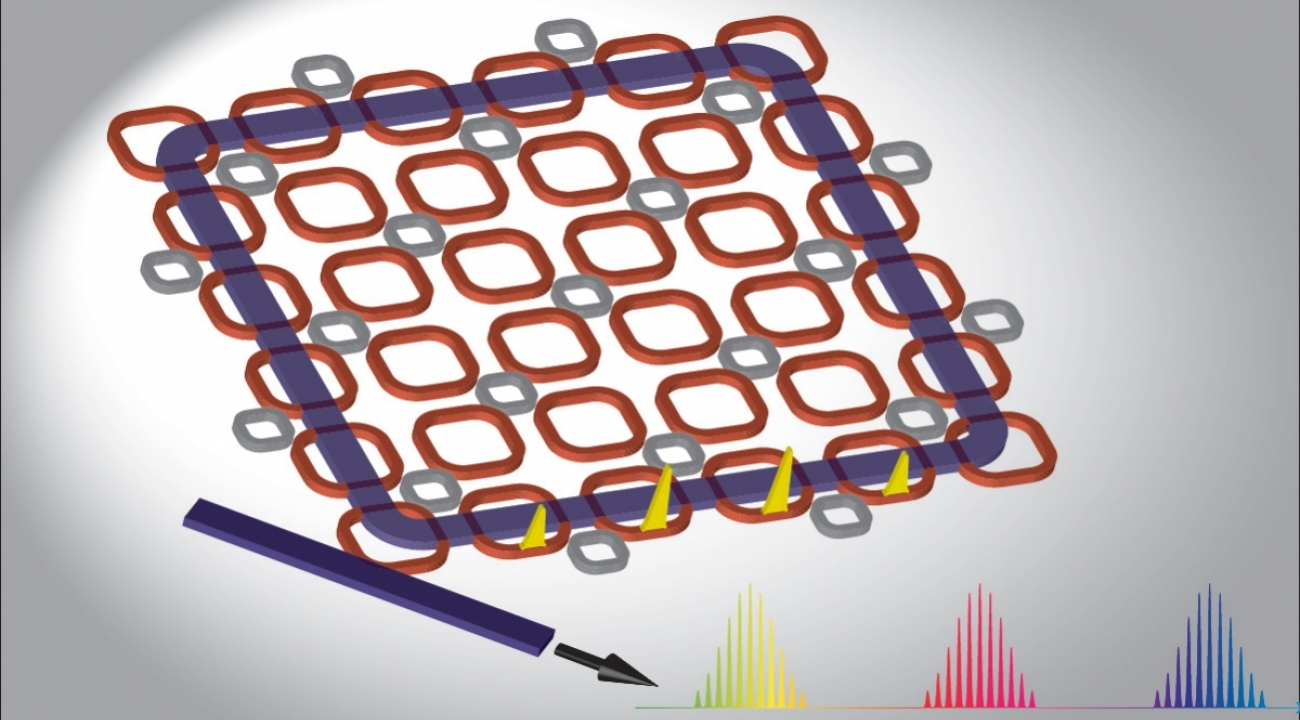
An electromagnetic enclosure can be characterized by its scattering parameters, which are voltage to voltage transfer functions defining the behavior of transmission and reflection between inputs and outputs. One method of dynamically changing the scattering parameters is to install a programmable metasurface inside the cavity. A programmable metasurface consists of multiple unit cells, each of which can modify its reflection coefficient, allowing the direction of reflected rays to be adjusted on-the-fly. Conceptual overview of the metasurface-enabled cavity as a closed-loop system. The cavity S parameters (scattering parameters) are measured with a network analyzer and passed to a controller that updates the metasurface elements with a new set of commands. The controller can generate cold spots at port 2 at an arbitrary set of frequencies, or drive candidate S-matrix eigenvalues towards the origin, and includes a stochastic iterative optimization algorithm. The three ports allow additional angular and spatial diversity to be added at the inputs. The inset shows a closeup view of one of the metasurface unit cells.Conceptual overview of the metasurface-enabled cavity as a closed-loop system. The cavity S parameters (scattering parameters) are measured with a network analyzer and passed to a controller that updates the metasurface elements with a new set of commands. The controller can generate cold spots at port 2 at an arbitrary set of frequencies, or drive candidate S-matrix eigenvalues towards the origin, and includes a stochastic iterative optimization algorithm. The three ports allow additional angular and spatial diversity to be added at the inputs. The inset shows a closeup view of one of the metasurface unit cells.

Researchers in the Wave Chaos Group at the University of Maryland, College Park (UMD) have used this approach to create on-demand coldspots, or nulls in transmission, effectively generating an electromagnetic cone of silence. Their work, published on December 29 in Physical Review Research, used a binary tunable metasurface manufactured by the Johns Hopkins University Applied Physics Laboratory. The relationship between commands and cavity scattering parameters is extremely complex, so simple linear techniques fail to converge. The team, led by electrical and computer engineering Ph.D. student Benjamin Frazier, developed an efficient stochastic algorithm and experimentally demonstrated the ability to generate coldspots at arbitrary frequencies, with arbitrary bandwidths, and even when driving multiple inputs.

“Chaotic microwave cavities are extremely useful as surrogates to probe the behavior of electromagnetic waves in larger complicated enclosures and are used in many of the research projects being investigated both by our group and collaborators at facilities such as the Naval Research Lab,” said Frazier. “The ability to dynamically modify the cavity in a very detailed and controllable manner is a significant advancement towards harnessing waves as they propagate through these rich scattering environments.”

In addition, they showed the ability to induce coherent perfect absorption states inside the cavity. Coherent perfect absorption is a special condition inside the cavity where all incoming energy injected into the cavity is absorbed and has great promise as a method to enable long range wireless power transfer.

Other authors of the paper include UMD Electrical and Computer Engineering and Physics Professors Thomas M. Antonsen,  Edward Ott and  Steven M. Anlage.

DOI: https://doi.org/10.1103/PhysRevResearch.2.043422

Original story: https://ece.umd.edu/news/story/umd-researchers-create-ondemand-cold-spots-to-generate-electromagnetic-cone-of-silence 

A Frankenstein of Order and Chaos

Normally the word “chaos” evokes a lack of order: a hectic day, a teenager’s bedroom, tax season. And the physical understanding of chaos is not far off. It’s something that is extremely difficult to predict, like the weather. Chaos allows a small blip (the flutter of a butterfly wing) to grow into a big consequence (a typhoon halfway across the world), which explains why weather forecasts more than a few days into the future can be unreliable. Individual air molecules, which are constantly bouncing around, are also chaotic—it’s nearly impossible to pin down where any single molecule might be at any given moment.

Now, you might wonder why anyone would care about the precise location of a single air molecule. But you might care about a property shared by a whole bunch of molecules, such as their temperature. Perhaps unintuitively, it is the chaotic nature of the molecules that allows them to fill up a room and reach a single temperature. The individual chaos ultimately gives rise to collective order.

Being able to use a single number (the temperature) to describe a bunch of particles bouncing around in some crazy, unpredictable way is extremely convenient, but it doesn’t always happen. So, a team of theoretical physicists at JQI set out to understand when this description applies.Researchers at JQI have discovered a quantum system that is a hybrid of order and chaos. (Credit: geralt/Pixabay)Researchers at JQI have discovered a quantum system that is a hybrid of order and chaos. (Credit: geralt/Pixabay)

"The ambitious goal here is to understand how chaos and the universal tendency of most physical systems to reach thermal equilibrium arises from fundamental laws of physics," says Victor Galitski, a Fellow of the Joint Quantum Institute (JQI).

As a first step towards this ambitious goal, Galitski and two colleagues set out to understand what happens when many particles, each of which is chaotic on its own, get together. For example, the motion of a single puck in an air hockey game, bouncing uninterrupted off the walls, is chaotic. But what happens when a lot of these pucks are let loose onto the table? And furthermore, what would happen if the pucks obey the rules of quantum physics?

In a paper published recently in the journal Physical Review Letters(link is external), the team studied this air hockey problem in the quantum realm. They discovered that the quantum version of the problem (where pucks are really quantum particles like atoms or electrons) was neither ordered nor chaotic, but a little bit of both, according to one common way of measuring chaos. Their theory was general enough to describe a range of physical settings, including molecules in a container, a game of quantum air hockey, and electrons bouncing around in a disordered metal, such as copper wire in your laptop.

“We always thought it was a problem that’s been solved a long time ago in some textbook,” says Yunxiang Liao, a JQI postdoc and the first author on the paper. “It turns out it's a more difficult problem than we imagined, but the results are also more interesting than we imagined.”

One reason this problem has remained unsolved for so long is that once quantum mechanics enters the picture, the usual definitions of chaos don’t apply. Classically, the butterfly effect—tiny changes in initial conditions causing drastic changes down the line—is often used as a definition. But in quantum mechanics, the very notion of initial or final position doesn’t quite make sense. The uncertainty principle says that the position and speed of a quantum particle can’t be precisely known at the same time. So, the particle’s trajectory isn’t very well defined, making it impossible to track how different initial conditions lead to different outcomes.

One tactic for studying quantum chaos is to take something classically chaotic, like a puck bouncing around an air hockey table, and treat it quantum mechanically. Surely, the classical chaos should translate over. And indeed, it does. But when you put more than one quantum puck in, things become less clear.

Classically, if the pucks can bounce off each other, exchanging energy, they will eventually all reach a single temperature, exposing the collective order of the underlying chaos. But if the pucks don’t bump into each other, and instead pass through each other like ghosts, their energies will never change: the hot ones will stay hot, the cold ones will stay cold, and they’ll never reach the same temperature. Since the pucks don’t interact, collective order can’t emerge from the chaos.

The team took this game of ghost air hockey into the quantum mechanical realm expecting the same behavior—chaos for one quantum particle, but no collective order when there are many. To check this hunch, they picked one of the oldest and most widely used (albeit not the most intuitive) tests of quantum chaos.

Quantum particles can’t just have any energy, the available levels are ‘quantized,’ which basically means they are restricted to particular values. Back in the 1970’s, physicists found that if the quantum particles behaved in predictable ways, their energy levels were completely independent of one another—the possible values didn’t tend to bunch up or spread out, on average. But if the quantum particles were chaotic, the energy levels seemed to avoid each other, spreading out in distinctive ways. This energy level repulsion is now often used as one of the definitions of quantum chaos.

Since their hockey pucks didn’t interact, Liao and her collaborators weren’t expecting them to agree on a temperature, meaning that they wouldn’t see any indications of the underlying single-puck chaos. The energy levels, they thought, would not care about each other at all.

Not only did they find theoretical evidence of some level repulsion, a hallmark of quantum chaos, but they also found that some of the levels tended to bunch together rather than repel, a novel phenomenon that they couldn’t quite explain. This deceptively simple problem turned out to be neither ordered nor chaotic, but some curious combination of the two that hadn’t been seen before.

The team was able to uncover this hybrid using an innovative mathematical approach. “In previous numerical studies, researchers were only able to include 20 or 30 particles,” says Liao. “But using our mathematical approach from random matrix theory, we could include 500 or so. And this approach also allows us to calculate the analytic behavior for a very large system.”

Armed with this mathematical framework, and with piqued interest, the researchers are now extending their calculations to gradually allow the hockey pucks to interact little by little. "Our preliminary results indicate that thermalization may happen via spontaneous breaking of reversibility—the past becomes mathematically distinct from the future,” says Galitski. “We see that small disturbances get exponentially magnified and destroy all remaining signatures of order. But this is another story."

Story by Dina Genkina

In addition to Liao and Galitski, Amit Vikram, a JQI graduate student in physics at UMD, was an author on the paper.

Reference Publication
Research Contact
Victor Galitski This email address is being protected from spambots. You need JavaScript enabled to view it.
(link sends e-mail)
Yunxiang Liao This email address is being protected from spambots. You need JavaScript enabled to view it.
(link sends e-mail)
Original story: https://jqi.umd.edu/news/frankenstein-order-and-chaos

Enhanced Frequency Doubling Adds to Photonics Toolkit

The digital age has seen electronics, including computer chips, shrink in size at an amazing rate, with ever tinier chips powering devices like smartphones, laptops and even autonomous drones. In the wake of this progress, another miniature technology has been gaining steam: integrated photonics.

Photons, which are the quantum particles of light, have some advantages over electrons, the namesakes of electronics. For some applications, photons offer faster and more accurate information transfer and use less power than electrons. And because on-chip photonics are largely built using the same technology created for the electronics industry, they carry the promise of integrating electronics and photonics on the same chip.

Tiny photonic chips have already been adopted in many places, including telecommunications networks (think fiber optic internet) and large data centers (think interfacing fiber-optics with electronics). Other industries are on the precipice of benefitting from photonics, with self-driving car makers developing(link is external) light-based radar chips. However, many tools that are well-established in traditional optics—things that use lasers, lenses and other bulky equipment—do not yet have a compact photonic analogue. For futuristic tools like light-based quantum computers or portable optical clocks, more work remains to package everything together.

Now, researchers at the Joint Quantum Institute (JQI) have added a new tool to the photonics toolkit: a way to use silicon, the native material for much of digital electronics and photonics, to efficiently double the frequency of laser light. By combining two existing techniques, the team achieved a frequency doubling efficiency 100 times greater than previously experiments with silicon compounds. They detailed their results in a paper published in the journal Nature Photonics(link is external).

Light waves are made up of photons, but they also carry a frequency. Our eyes see a small fraction of these frequencies as the colors of the rainbow, but microwaves, x-rays and radio waves (among others) also inhabit this spectrum. Doubling the frequency of light is one way to convert between these different ranges. In the new work, the team demonstrated a doubling of infrared light—commonly used in optical telecommunications—to red light, the language of very precise atomic clocks.

Frequency doubling is one effect that can occur when light interacts with the medium it’s traveling through, be it air, water or silicon. Depending on the properties of these materials, a little bit of the light can be doubled, tripled, or, in extreme cases, multiplied to even higher degrees, like a musical note also generating a bit of sound one, two, or several octaves up. By choosing the right material, and illuminating it in the right way, researchers can get to the harmonic they need.

Unfortunately, silicon and silicon compounds—the materials of choice for routing light on a chip because of the maturity of silicon manufacturing and the ease of integrating with elA new photonic chip can double the frequency (f) of incoming light using a circular ring 23 microns across. The ring is tailored to generate and hold light at the input frequency and at its second harmonic (2f)—just like piano strings or organ tubes can host harmonics of a single tone. The color indicates crests and troughs of the light field, similar to a piano string’s displacement pattern when it rings. (Credit: Xiyuan Lu/NIST and UMD)A new photonic chip can double the frequency (f) of incoming light using a circular ring 23 microns across. The ring is tailored to generate and hold light at the input frequency and at its second harmonic (2f)—just like piano strings or organ tubes can host harmonics of a single tone. The color indicates crests and troughs of the light field, similar to a piano string’s displacement pattern when it rings. (Credit: Xiyuan Lu/NIST and UMD)ectronics—don’t intrinsically support frequency doubling. The crystal structure is too uniform, meaning it looks the same in all directions. This prohibits the doubling effect, which relies on electrons in the material shifting one way more than another under the influence of light. But once light is confined to a tiny trace on a chip, things become a little less uniform: After all, the air is always nearby, and it doesn’t look at all like a silicon crystal. So, a tiny amount of frequency doubled light does get generated, but usually it is not enough to be useful.

In the new work, a team led by Adjunct Professor Kartik Srinivasan, a Fellow of the National Institute of Standards and Technology (NIST), and NIST and UMD postdoctoral researcher Xiyuan Lu, combined two previously explored techniques to build on this tiny effect, generating 100 times more frequency doubled light than any previous silicon experiments. Additionally, their doubling occurred with an efficiency of 22%, appreciable enough to be useful in applications.

The first trick was to capture the light in a resonator, making the light go round and round and triggering the tiny doubling effect over and over again. To achieve this, the researchers first routed near-infrared laser light into an optical fiber. The fiber then shot the light into a silicon nitride waveguide printed on a silicon chip. This waveguide led to another waveguide, which was wrapped into a circle just 23 microns in diameter. The circular resonator, which was engineered to capture the incoming light and circulate it around, allowed a tiny bit of frequency doubling to happen over and over again. Another straight waveguide, on the other edge of the resonator, was tuned to carry away the frequency-doubled light.

The second trick was to make the silicon less uniform by biasing it with an electric field. Luckily, no external field was actually needed—the tiny amount of frequency doubled light, combined with the original infrared pump light, caused the electrons in the resonator to gather at the edges, creating a constant electric field. This field greatly enhanced the frequency doubling capacity of the silicon nitride.

“It’s a feedback process,” says Srinivasan, “because a little bit of frequency doubled light and pump light start to create the constant electric field, making the frequency doubling process stronger, which in turn creates more frequency doubled light. So both the pump light and the frequency doubled light are circulating around in this ring, and there’s this huge ability to take this thing that started out as extremely weak, and then actually make it a pretty strong effect.”

Getting both of these effects to work in the same device wasn’t easy. Not only does the resonator ring need to be exactly the right size to trap the pump and frequency doubled light, the light also needs to stack up in the right way in the resonator. To achieve this, detailed simulations and precise manufacturing in a clean room are necessary. But once such an accurate device is fabricated, all you need to do is send in pump light, and observe frequency doubled light at the output.

“To enable efficient interaction between light and the material, light of different colors has to live a long time and also move at exactly the same speed,” says Lu, “Our device implements these two key factors into photo-induced frequency doubling, which significantly boosts the power efficiency of this process.”

This device is another step in a long quest to achieve a portable, ultra-precise atomic clock. “These optical clocks are these amazing timekeeping devices, but usually they're in a big lab,” says Srinivasan. “If it could be in a small package it could go on cars or drones or other vehicles. Timing underlies a lot of important navigation applications, and for the most part, now, people rely upon GPS signals. But there are all sorts of possibilities that there might be something in the way, and you can’t acquire those signals, or somebody spoofs the signal. So, having portable timing instruments that could really give you accurate and precise time for long stretches before you need a synchronization signal from GPS is meaningful.”

Although it’s not the star of the show, frequency doubling is a necessary component in optical atomic clocks. These clocks produce an extremely regular beat, but at optical frequencies—hundreds of trillions of light field oscillations per second. Conventional electronics can’t interface with that signal directly, so to bring this precision down to an intelligible frequency (mere billions of oscillations per second) scientists use frequency combs—laser sources with frequency ‘teeth’ at perfectly regular intervals, an invention that won the 2005 Nobel Prize in physics(link is external).

To be useful, these frequency combs need to be calibrated—each tooth in the comb needs to be labeled with a specific frequency value. The simplest and most common way to calibrate them is to take the lowest tooth in the comb, frequency double it, and compare to the highest tooth: this gives the frequency of the lowest tooth. Along with a simple measurement of the spacing between teeth, scientists can use this to deduce the exact frequency of each tooth.

Recently, several pieces of the on-chip atomic clocks, including tiny atomic vapor cells and on-chip frequency combs, have been achieved in silicon-based photonics. However, the frequency doubling calibration was previously done with bulky optics or using materials that are less compatible with silicon. “At least conceptually,” says Srinivasan, “we’re one step closer to a calibrated frequency comb in a really compact package. There's still work to be done to really be able to put these things together, but we’re closer to a compact optical atomic clock than we were before.”

Original story by Dina Genkina: https://jqi.umd.edu/news/enhanced-frequency-doubling-adds-photonics-toolkit

In addition to Srinivasan and Lu, this paper had 3 additional co-authors: Gregory Moille, a postdoctoral researcher at JQI and NIST; Ashutosh Rao, a postdoctoral researcher in chemistry and biochemistry at UMD and NIST; and Daron A. Westly, a research scientist at NIST

Research Contact: Kartik Srinivasan (This email address is being protected from spambots. You need JavaScript enabled to view it.)

UMD-NIST Self-Directing AI System Discovers New Material

When the words “artificial intelligence” (AI) come to mind, your first thoughts may be supercomputers, or robots that perform tasks without assistance from humans. Now, a multi-institutional team led by researchers from the University of Maryland (UMD) and National Institute of Standards and Technology (NIST) working with collaborators at Stanford University, University of Washington, University of Pennsylvania, and Duke University have accomplished something not too far off. They developed an AI algorithm called CAMEO that discovered a useful new material without requiring additional training from scientists. The AI system could help reduce the amount of trial-and-error time scientists spend in the lab, while maximizing productivity and efficiency in their research.

The research team published their work on CAMEO in Nature Communications on November 24, 2020.

In the field of materials science, scientists seek to discover new materials that can be used in specific applications. “For example, we are always looking are new quantum materials which can be used for quantum computers and sensors,” said physics affiliate Ichiro Takeuchi, a professor of materials science and engineering and member of the Quantum Materials Center (QMC) at UMD.

But finding such new materials usually takes a large number of coordinated experiments and time-consuming theoretical searches. If a researcher is interested in how a material’s properties vary with different temperatures, then that may mean 10 experiments at 10 different temperatures. Temperature, however, is just one parameter. If there are five parameters, each with 10 values, then that researcher must run the experiment 10 x 10 x 10 x 10 x 10 times, a total of 100,000 experiments. It’s nearly impossible for a researcher to run that many experiments via brute force due to the years or decades it may take.

That’s where CAMEO comes in. Short for Closed-Loop Autonomous System for Materials Exploration and Optimization, CAMEO can ensure that each experiment maximizes the scientist’s knowledge and understanding, skipping over experiments that would give redundant information. Helping scientists reach their goals faster with fewer experiments also enables  labs to use their limited resources more efficiently. But how is CAMEO able to do this?

Method Behind the Process

Active learning is a machine learning technique in which computer programs can access data and process it themselves, automatically updating the knowledge and deciding the optimum sequence of information acquisition. This is the basis for CAMEO, a self-learning AI that uses prediction and uncertainty to determine which experiment to try next.

As implied by its name, CAMEO looks for a useful new material by operating in a closed loop: it determines which experiment to run on a material, does the experiment, and collects the data. It can also ask for more information, such as the crystal structure of the desired material, from the scientist before running the next experiment, which is informed by all past experiments achieved in the loop.  

“The key to our experiment was that we were able to unleash CAMEO on a combinatorial library where we had made a large array of materials with all different compositions,” said Takeuchi. “In a usual combinatorial study, every material in the array would have been measured one by one to look for the compound with the best properties. Depending on the property of interest, even with a fast measurement setup, that can take a long, long time. With CAMEO, it only took a small fraction of total number of measurements to home in on the best material.”

The AI is also designed to contain knowledge of key principles, some of which includes knowledge of past simulations and lab experiments, how the equipment works, and physical concepts. For example, the researchers armed CAMEO with the knowledge of phase diagrams, which describes how the arrangement of atoms in a material changes with chemical composition and temperature.

Understanding how atoms are arranged in a material is important in determining its properties such as how hard, or how electrically-insulating it is, and how well it is suited for a specific application.

“The AI is unsupervised,” said NIST researcher, Aaron Gilad Kusne. “Many types of AI need to be trained or supervised. Instead of asking it to learn physical laws, we encode them into the AI. You don’t need a human to train the AI.”

One of the best ways to figure out the structure of a material is by bombarding it with x-rays, in a technique called x-ray diffraction. By identifying the angles at which the x-rays bounce off, scientists determine how atoms are arranged in a material, enabling them to figure out its crystal structure. However, a single in-house x-ray diffraction experiment can take an hour or more. At a synchrotron facility, a large machine the size of a football field that accelerates electrically charged particles at close to the speed of light, this process can take 10 seconds, because the fast-moving particles emit large numbers of x-rays. This is the method used in the study at the Stanford Synchrotron Radiation Lightsource.

CAMEO then decides which material composition to study next and focuses the x-rays on the appropriate part of the sample where that composition exists, to investigate its atomic structure. With each new iteration, CAMEO learns from past measurements and identifies the next material to study.  This allows the AI to explore how a material’s composition impacts its structure and use this information to find the best material for the task.

“Think of this process as trying to make the perfect cake,” Kusne said. “You’re mixing different types of ingredients, flour, eggs, or butter, using a variety of recipes to make the best cake. With the AI, it’s searching through the ‘recipes’ or experiments to determine the best composition for the material.”

That is how CAMEO discovered the material  which the group shortened to GST467. CAMEO was provided with 177 potential materials to investigate, covering a large range of compositional recipes. To arrive at this material, CAMEO performed 19 different experimental cycles, which took 10 hours, compared to the estimated 90 hours it would have taken a scientist with the full set of 177 materials.

The New Material

The material is composed of three different elements (germanium, antimony and tellurium, Ge-Sb-Te) and is a phase-change memory material, that is, it changes its atomic structure from crystalline (solid material with atoms in designated, regular positions) to amorphous (solid material with atoms in random positions) when quickly melted by applying heat. This type of material is used in memory applications such as data storage. Although there are infinite composition variations possible in the Ge-Sb-Te alloy system, the new material GST467 discovered by CAMEO is optimal for phase-change applications.

The research team wanted CAMEO to find the best Ge-Sb-Te alloy, one that had the largest difference in optical contrast between the crystalline and amorphous states. Optical contrast, for example on a DVD disc, allows a scanning laser to read the disc by distinguishing between regions that have high or low reflectivity. They found that GST467 has twice the contrast for a phase change material compared to GST225 or , a well-known material that’s commonly used for DVDs. The larger contrast enables the new material to outperform the old material by a significant margin.

The key part of the experiments was conducted at the Stanford National Accelerator Laboratory (SLAC) at Stanford University, for the U.S. Department of Energy Office of Science. SLAC researchers helped oversee the experiments run by CAMEO.

UMD researchers provided the materials used in the experiments and researchers at the University of Washington – led by Electrical and Computer Engineering Professor, Mo Li – demonstrated the new material in a patterned phase-change memory device. 

The new material GST467 has applications for photonic switching devices, which control the direction of light in a circuit. They can also be applied in neuromorphic computing, a field of study focused on developing devices that emulate the structure and function of neurons in the brain, opening possibilities for new kinds of computers as well as other applications such as extracting useful data from complex images.

The work also involved collaboration with electron microscopists at NIST who performed high-resolution microscopy to understand the microstructure of the newly found compound.

Applications to other Materials

The researchers believe CAMEO can be used for other types of materials, such as high-temperature alloys and quantum materials. The code for CAMEO is open source and will be freely available for use by scientists and researchers.

There had been other reports of closed-loop materials and chemistry optimization work. The critical distinguishing feature of the present work with CAMEO is that it was used to discover a novel solid state material whose functionality is encoded in the composition-structure-property relationship of crystalline materials, and as such, the algorithm was able to navigate the course of discovery path by tracking the structural origins of materials functionalities.

One application of CAMEO is minimizing experimental costs since using synchrotron facilities requires time, researchers need a written proposal to use the equipment, and money. But with AI running the experiments, they can be carried out quicker. Researchers estimate a 10-fold reduction in time for experiments using CAMEO since the number of experiments performed can be cut by one tenth. Because the AI is running the measurements, collecting data and performing the  analysis, this also reduces the amount of knowledge a researcher needs to run the experiment. All the researcher must focus on is running the AI.

Another potential benefit is providing the ability to work remotely for scientists. “This opens up a wave of scientists to still work and be productive without actually being in the lab,” said SLAC researcher Apurva Mehta. This could mean if scientists wanted to work on research involving contagious diseases or viruses, such as COVID-19, they could do so safely and remotely while relying on the AI to conduct the experiments in the lab.

Researchers are continuing to improve the AI and try to make the algorithms capable of solving ever more complex problems. “The ultimate goal is to incorporate synthesis of crystalline materials in the closed loop – this is particularly hard since standard synthesis tools of crystalline functional materials are not equipped with measurement capabilities,” said Takeuchi. “That calls for some novel hardware integration as well as advances in AI. The future is robot materials science.”  

Original story: https://mse.umd.edu/news/story/umdnist-selfdirecting-ai-system-discovers-new-material